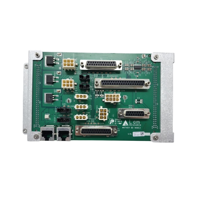
1. Product Overview (810-800256-005)
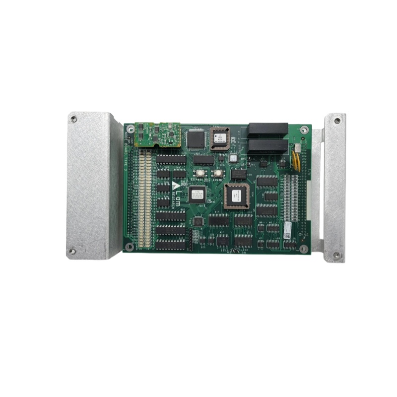
The Lam Research 810-800256-005 is a dedicated control and interface board assembly designed by Lam Research for its industry-leading 810-series semiconductor wafer fabrication equipment. Officially designated asNODE BOARD, TYPE 3, this component functions as a core management node within the equipment’s distributed control architecture.
Deployed in highly complex plasma etching and chemical vapor deposition (CVD) systems, the board operates as an independent subsystem controller. It undertakes critical tasks including electrostatic chuck (ESC) temperature regulation, pneumatic valve bank control, and bidirectional communication coordination with key peripheral devices such as radio frequency (RF) generators and vacuum gauges. Leveraging robust signal processing and routing capabilities, the 810-800256-005 ensures precise command transmission between the main controller and execution units, as well as real-time feedback of operational status data. It serves as a core component that guarantees high process repeatability and stable equipment operation.
Manufactured with industrial-grade materials and processes optimized for semiconductor cleanroom environments, this node board supports a wide operating temperature range of 10°C to 40°C, enabling long-term stable performance under the constant-temperature and constant-humidity stringent conditions of semiconductor FAB facilities. As a complete Printed Circuit Board Assembly (PCBA), it integrates a microprocessor, memory modules, communication interfaces, and multiple I/O circuits to form a compact, fully functional micro control unit.
Featuring a modular design, the board supports rapid replacement in the event of board-level failures. This design significantly reduces the Mean Time To Repair (MTTR), minimizes equipment downtime, and delivers indispensable support for high-throughput wafer production line operations.
2. Product Specifications
|
Parameter Item
|
Specification Value
|
|
Product Model
|
810-800256-005
|
|
Manufacturer
|
Lam Research
|
|
Product Type
|
Node Board, Type 3 (Controller & Interface Board)
|
|
Functional Description
|
Subsystem control, signal routing, and power distribution
|
|
Compatible Platform
|
Lam Research 810-series plasma etching & deposition systems
|
|
Application Environment
|
Class 1000 or higher cleanroom / Semiconductor FAB environment
|
|
Operating Temperature
|
10°C ~ 40°C
|
|
Typical Logic Voltage
|
24 VDC (subject to specific system configuration)
|
|
Compliance Standards
|
CE, RoHS
|
3. Structure & Composition
The Lam Research 810-800256-005 adopts a high-integration and functional partitioned design, conforming to modern semiconductor equipment electronic module design standards. Its physical carrier is an industrial-standard multi-layer Printed Circuit Board (PCB) fabricated with high Tg FR-4 substrate, which delivers excellent dimensional stability and consistent electrical performance under temperature fluctuations.
Surface components are scientifically partitioned into three core functional units to form a closed-loop information processing and control system:
3.1 Core Processor & Logic Unit
Equipped with an on-board Microcontroller Unit (MCU) or Field Programmable Gate Array (FPGA) and supporting memory chips, this unit undertakes core tasks including control logic execution, communication protocol processing, and operational data calculation.
3.2 Signal Conditioning & I/O Interface Unit
Composed of isolated components, operational amplifiers, and digital isolators, this unit amplifies and filters analog signals collected from external sensors (thermocouples, pressure gauges, etc.), converts digital signal levels, and provides electrical isolation. It effectively guarantees signal integrity and anti-interference capability in complex industrial environments.
3.3 Power Management Unit
This unit performs DC-DC conversion on the input voltage (24 VDC) from the equipment backplane, supplying stable and purified operating power for all on-board chips and circuits. The coordinated operation of the three units enables comprehensive and precise subsystem control.
4. Core Features & Advantages
4.1 High Reliability & Native Compatibility
As an original Lam Research factory component, the 810-800256-005 is designed and manufactured in full compliance with the reliability standards of complete 810-series equipment. All electronic components undergo strict screening, and the PCB layout and stacking design are optimized for Signal Integrity (SI) and Electromagnetic Compatibility (EMC). It maintains stable operation even in high-interference plasma etching environments. As a highly customized component, it achieves plug-and-play compatibility with matched Lam equipment models in terms of physical dimensions, electrical interfaces, communication protocols, and software drivers, eliminating compatibility risks caused by third-party alternative parts.
4.2 Modular Architecture Optimizes Maintenance Efficiency
The board features a fully modular structure and connects with equipment backplanes and wiring harnesses via standardized connectors. For subsystem communication failures or control anomalies related to the node board, technicians can quickly locate and replace the component. This board-level replacement strategy reduces MTTR from hours to minutes, minimizing production loss caused by equipment downtime and significantly improving the Overall Equipment Effectiveness (OEE) of wafer fabs.
4.3 Powerful System Control & Coordination Capability
As a critical node of the distributed control system, the board independently manages multiple dedicated subsystems, such as the high-precision temperature control loop of electrostatic chucks (ESCs) for wafer temperature regulation. The functional decentralization design reduces the computing load of the main controller, improving the real-time response capability and parallel processing efficiency of the entire equipment system.
5. Application Fields
The Lam Research 810-800256-005 is exclusively applied to core front-end processes of semiconductor wafer manufacturing, including plasma etching and thin-film deposition. It is widely integrated into Lam Research mainstream platforms such as Kiyo®, Versys®, and 2300® series etching equipment, as well as supporting Chemical Vapor Deposition (CVD) and Atomic Layer Deposition (ALD) systems for logic chips (CPU, GPU) and memory chips (DRAM, 3D NAND).
Its core application scenarios cover two key dimensions:
First, as a dedicated subsystem controller, it precisely regulates wafer temperature with an accuracy of ±0.1°C by controlling heaters and cooling gas flow, ensuring consistent etching rate and process selectivity. Second, as a communication relay hub, it bridges the main control computer with various chamber sensors (pressure gauges, endpoint detectors) and actuators (pneumatic valves, handling robots), realizing real-time and reliable transmission of massive process data. It is a key component that ensures process stability, repeatability, and high yield in advanced chip manufacturing.
6. Related Products
- 810-802902-207: A complementary electronic module of the Lam Research 810 series, defined as the mainboard node. It focuses on system-level main control and data aggregation functions, forming a collaborative control system with the Type 3 node board (810-800256-005).
- 810-800082-043: A strictly certified original factory component in the Lam Research equipment ecosystem, applicable to RF matchers, gas circuit modules, or dedicated circuit boards, featuring exclusive factory matching and systematic compatibility.
- 810-102361-222: A high-value core spare part for 810-series etching equipment, covering electrostatic chuck (ESC) components, chamber assemblies, gas modules, and RF electrode accessories.
- 810-370141-001: A PCB interlock board responsible for processing safety-related control signals. It supports the equipment safety interlock system and ensures all operational actions comply with preset safety specifications.
7. Installation & Maintenance
7.1 Pre-Installation Preparation
Installation of the 810-800256-005 must be performed by Lam Research trained and authorized professionals in a strictly controlled cleanroom environment. Before installation, completely power off the equipment and implement Lockout/Tagout (LOTO) procedures to release all residual energy. Operators must wear full cleanroom apparel and complete ESD protection equipment (ESD wristband & grounding wire).
Align the board with equipment guide rails and backplane connectors, insert it evenly and smoothly until the locking mechanism clicks into place to ensure full pin engagement. Direct contact with on-board components and gold fingers is strictly prohibited to avoid electrostatic damage and surface contamination.
7.2 Maintenance Guidelines
Daily maintenance focuses on equipment log monitoring and preventive replacement. During periodic maintenance, visually inspect the board surface and connectors for dust accumulation, corrosion, or burn marks. For subsystem-related alarm errors and communication anomalies, prioritize the 810-800256-005 as a key inspection object.
Thanks to the rapid replacement design, faulty boards can be replaced in a short time with ultra-low MTTR. After replacement, run official equipment diagnostic programs (I/O loop testing, etc.) to verify functional integrity, and perform standardized calibration procedures per the official manual to restore optimal production status.
8. Product Warranty & Support
We fully recognize that any equipment failure in semiconductor manufacturing may cause substantial production losses. All supplied Lam Research 810-800256-005 components are sourced from certified reliable supply chains and undergo strict visual and functional testing.
We provide a 12-month functional warranty from the date of delivery, covering non-artificial operational failures. Our professional technical team delivers one-stop full-cycle services, including pre-sales model matching confirmation, in-sales technical consultation, and after-sales fault troubleshooting, ensuring stable and worry-free production operation for customers.
9. Product Overview (810-802902-207)
The Lam Research 810-802902-207 is an advanced electronic module developed by Lam Research for high-end semiconductor wafer fabrication equipment, commonly known as the Mainboard Node in the industry.
Different from the 810-800256-005 (Type 3 Node Board) which focuses on independent subsystem control, the 810-802902-207 serves as the core system-level data convergence and information interaction hub. It connects core processors, memory modules, and various functional expansion cards, providing high-speed and high-reliability electrical connection and signal transmission channels for the entire equipment system.
Deployed in high-value etching and deposition equipment, this mainboard node synchronizes the operating rhythms of all subsystems including RF generators, gas flow control units, vacuum systems, and wafer handling robots. It coordinates complex process step sequences and acts as the central nerve center of the entire equipment control system, guaranteeing overall systematic coordination and stable process operation.