Product Overview
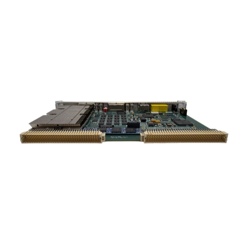
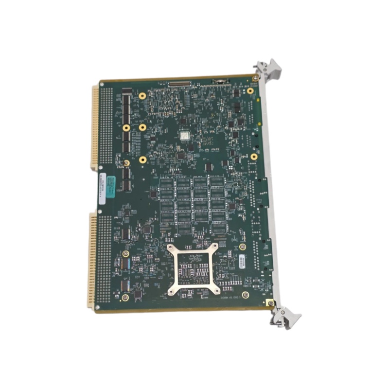
The Lam Research 605-A02119-001 is a core component of the gas distribution system engineered for high-density plasma etching and chemical vapor deposition (CVD) processes. It serves as a vital part of the reaction chamber gas injection and isolation subsystem in Lam Research semiconductor manufacturing equipment. Its core function is to achieve precise injection, uniform distribution of process gases, and reliable vacuum sealing isolation of key areas at the top or sidewall of the reaction chamber. As a critical sealing and distribution element in the gas showerhead system and gas injection module, it enables reaction gases to enter the plasma reaction zone with preset flow field distribution and flow rate ratios, directly determining etching uniformity, deposited film thickness consistency, and the smooth discharge of reaction by-products.
Fabricated from corrosion-resistant and high-purity specialty materials via precision machining, the Lam Research 605-A02119-001 features a structural design optimized to withstand the harsh chemical environments and thermal cycling stresses inherent to semiconductor processes. The component surface undergoes specialized passivation or coating treatment to minimize particle generation and metal contamination risks. Integrated with precision micro-hole arrays, gas distribution channels, and sealing structures, it fits tightly with the chamber upper electrode and gas injection module, forming the final and most critical gas path for process gases traveling from the mass flow controller (MFC) to the wafer surface reaction zone. In modern 300mm wafer manufacturing, its machining accuracy and surface cleanliness level directly affect process yield and equipment mean time between cleans (MTBC), acting as a core hardware foundation for stabilizing advanced manufacturing processes and ensuring product consistency.
Product Specifications
|
Parameter Name
|
Parameter Value
|
|
Product Model
|
605-A02119-001
|
|
Manufacturer
|
Lam Research
|
|
Product Type
|
Gas Distribution Plate / Showerhead Component
|
|
Applicable Processes
|
Plasma Etching, CVD/ALD Thin Film Deposition
|
|
Main Material
|
High-purity Aluminum Alloy / Stainless Steel (Anodized or Ni/PTFE coated surface)
|
|
Gas Distribution Mode
|
Multi-zone uniform distribution via micro-hole array
|
|
Sealing Structure
|
FFKM (Perfluoroelastomer) O-ring groove design
|
|
Operating Temperature Range
|
20°C to 200°C (subject to chamber process conditions)
|
|
Operating Pressure Range
|
1 mTorr to Atmospheric Pressure (Vacuum-compatible)
|
|
Surface Finish
|
Ra < 0.4 μm (gas-contacting area)
|
|
Particle Control Level
|
< 0.1 particles/cm² (tested after wet cleaning)
|
|
Physical Dimensions
|
Approx. 380mm (Diameter) × 15mm (Thickness), subject to chamber configuration
|
|
Installation Method
|
Bolt fastening installation on the top flange of the chamber
|
Structure and Composition
The internal structure and surface morphology of the Lam Research 605-A02119-001 embody a design concept that deeply integrates precision mechanical machining with semiconductor process requirements. The component adopts an overall disc or annular structure. Its process side (facing the wafer) is densely covered with micro-hole arrays arranged and optimized based on professional fluid dynamics models. The diameter, depth and distribution density of these micro-holes are non-uniform and zoned according to chamber internal electric field distribution and airflow simulation results, achieving excellent gas concentration uniformity across the entire wafer surface. Precision positioning pin holes and bolt mounting holes are machined on the outer edge of the component to ensure high repeat positioning accuracy during chamber installation, which is essential for maintaining process reproducibility.
A complex network of gas distribution channels is fabricated inside the component through multi-axis precision machining technology, connecting single or multiple gas inlets on the backside with hundreds to thousands of micro-holes on the front side. The channel design optimizes gas path resistance balance, ensuring that the airflow velocity at each micro-hole outlet maintains a preset proportional relationship under varying flow rate conditions. Sealing grooves are reserved on the back or side of the component for installing FFKM O-rings. When the component is compressed with the upper electrode or chamber cover plate, the O-ring deforms under the dual action of vacuum negative pressure and mechanical force, forming a reliable vacuum sealing interface that effectively isolates the reaction zone from the atmospheric environment and non-process areas. In addition, some versions of the 605-A02119-001 are equipped with built-in temperature control liquid channels. Cooperating with an external circulating temperature control system, it actively regulates the operating temperature of the gas distribution plate and inhibits condensation and accumulation of process by-products on the component surface.
Key Features and Advantages
1. Excellent Gas Distribution Uniformity and Process Consistency
The micro-hole array and gas flow channels of the Lam Research 605-A02119-001 are designed based on advanced computational fluid dynamics (CFD) simulation technology, ensuring ultra-high uniformity of reaction gas concentration and residence time on the wafer surface. The optimized airflow distribution synergizes perfectly with the chamber’s internal electric field distribution, stably maintaining ultra-high within-wafer uniformity of etching and deposition rates. Meanwhile, the high repeatability of component installation ensures highly consistent process conditions between individual wafers and production lots, effectively reducing wafer-to-wafer and lot-to-lot process deviations and providing a solid guarantee for large-scale mass production.
2. Superior Corrosion Resistance and Low Particle Generation
Semiconductor etching processes extensively adopt halogen-containing gases (such as CF₄, CHF₃, Cl₂, HBr) and their plasma products with strong chemical corrosiveness. This component is specially optimized in material selection and surface treatment to adapt to harsh process environments. The base material is manufactured via high-purity smelting and precision forging, with a dense and uniform anodized layer or professional anti-corrosion coating applied on the surface. It effectively resists chemical erosion by process gases and greatly extends the service life of the component. Furthermore, high-quality surface coating and rigorous machining processes restrain particle generation and shedding, minimizing risks of metal contamination and particle defects to meet the stringent defect density requirements of advanced-node semiconductor devices.
3. Precise Temperature Management and By-Product Control
Equipped with built-in temperature control channels, the 605-A02119-001 realizes active and precise regulation of operating temperature. By circulating heat-conducting media at a constant temperature, the component maintains a stable temperature field during processing, effectively suppressing the condensation and adhesion of high-boiling process by-products (such as polymers and salt sediments) on the gas distribution plate surface. This not only extends the chamber’s mean time between cleans (MTBC) and improves equipment utilization, but also reduces particle defects caused by by-product shedding, further boosting production yield.
Application Fields
The Lam Research 605-A02119-001 is widely applied in front-end semiconductor manufacturing processes, including dielectric etching, conductor etching, and plasma-enhanced chemical vapor deposition (PECVD). It serves as a standard configuration of the gas injection system for Lam Research 2300-series etchers, Flex-series deposition tools, and partial Exelan-series equipment, specifically tailored for advanced mass production of 300mm (12-inch) wafers.
In advanced logic chip manufacturing, it supports precise gas distribution for critical processes such as gate sidewall etching, low-k dielectric etching, and metal hard mask trenching. In 3D NAND flash memory production, it meets the ultra-high aspect ratio channel hole etching requirements for uniform gas distribution on the wafer surface.
This component solves two core pain points in semiconductor mass production. First, it realizes process uniformity for large-size wafers. With precision micro-hole array and flow channel design, it finely regulates gas concentration distribution and residence time from the center to the edge of 300mm wafers, ensuring consistent etching depth and critical dimension across the entire wafer surface. Second, it delivers long service life and low maintenance costs. The adoption of corrosion-resistant materials and active temperature control design significantly extends component service life, reduces chamber cleaning frequency, lowers consumable and comprehensive equipment maintenance costs for semiconductor manufacturers, and improves the overall equipment effectiveness (OEE) of production lines.