Product Overview
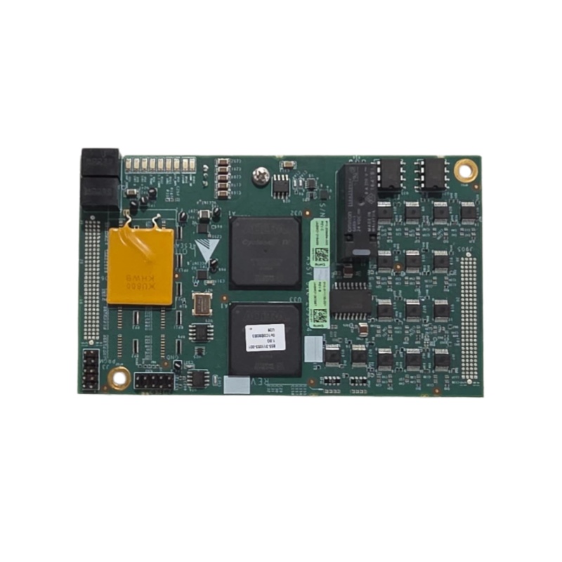
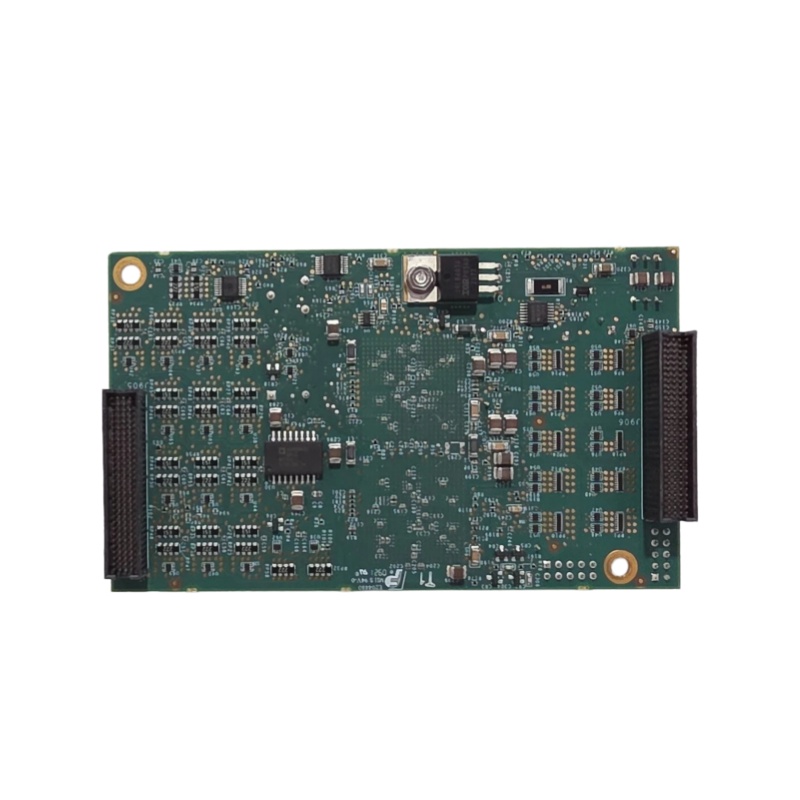
Lam Research 810-209684-005 is a dedicated electronic component designed by Lam Research for its wafer manufacturing equipment systems, classified as a Printed Circuit Board Assembly (PCBA). In highly complex plasma etching and chemical vapor deposition (CVD) systems, this module is primarily responsible for signal conditioning, interface conversion, and control of specific subsystems.
It accurately converts commands from the main controller into actions of underlying hardware, and preprocesses feedback signals from sensors (including temperature, pressure, and flow meters) before uploading them to the upper system. The stable operation of Lam Research 810-209684-005 is critical to ensuring overall equipment coordination and consistent process repeatability in semiconductor manufacturing.
Product Specifications
The technical specifications of this semiconductor spare part are summarized below based on universal industry technical characteristics:
|
Parameter Name
|
Parameter Value
|
|
Product Model
|
810-209684-005
|
|
Manufacturer
|
Lam Research
|
|
Product Type
|
Printed Circuit Board Assembly (PCBA) / Functional Module
|
|
Functional Description
|
Signal processing, interface conversion, and specific subsystem control
|
|
Compatible Equipment
|
Lam Research 810-series plasma etching and deposition systems
|
|
Application Environment
|
Class 1000 or higher cleanroom / Semiconductor Fab environment
|
|
Installation Method
|
Rack-mounted installation, docked with the backplane via dedicated connectors
|
|
Certification Standards
|
Compliant with SEMI S2, CE, RoHS and other semiconductor industry specifications
|
Structure and Composition
The physical carrier of Lam Research 810-209684-005 is a high-reliability multilayer Printed Circuit Board (PCB) manufactured with high-temperature-resistant and low-dielectric-loss substrates (such as high-Tg FR-4). Its internal structure consists of three core functional areas: core logic and processing unit, signal conditioning and I/O interface unit, and power management unit.
The core logic unit integrates Microcontroller Units (MCU), Complex Programmable Logic Devices (CPLD), or Field Programmable Gate Arrays (FPGA) to execute communication protocol processing, logical operation, and local control decision-making. The signal conditioning unit incorporates Analog-to-Digital Converters (ADC), Digital-to-Analog Converters (DAC), operational amplifiers, and digital isolators. It precisely amplifies and filters analog signals, isolates and level-shifts digital signals, and guarantees signal integrity and anti-interference performance.
The power management unit delivers stable and purified power supply to various circuits on the board through DC-DC converters. All functional units work collaboratively via well-designed PCB traces to realize the complete system functions of the 810-209684-005 module.
Key Features and Advantages
1. High Integration and Compact Design
Lam Research 810-209684-005 integrates multiple signal processing and interface conversion functions into a single compact module, effectively saving internal equipment space. It enables high-precision data exchange between the equipment main controller and underlying execution units, which is essential for maintaining ultra-high accuracy in wafer processing procedures.
2. High Reliability and Industry Standard Compatibility
As an original dedicated spare part of Lam Research, this board is designed and manufactured in strict accordance with stringent semiconductor equipment standards. It adopts high-quality electronic components and undergoes rigorous production and testing procedures to support continuous high-load operation in rigorous Fab environments, ensuring long-term operational stability and low failure rate.
3. Modular Architecture and Easy Maintainability
The module adopts standardized connectors for seamless docking with the equipment backplane. In case of failures, it supports rapid board-level replacement, which significantly reduces Mean Time To Repair (MTTR) and minimizes equipment downtime and production capacity losses.
Application Fields
Lam Research 810-209684-005 is mainly applied in the front-end manufacturing process of semiconductor chips. It is widely integrated into Lam Research etching and deposition equipment for the production of logic chips (CPU, GPU) and memory chips (DRAM, 3D NAND).
Serving as a professional signal processing and interface module, it connects the main control system with various chamber sensors (including pressure gauges, temperature sensors, and endpoint detectors) to ensure real-time and reliable transmission of massive process data. It also acts as a subsystem controller to manage specific functional modules such as gas flow control and temperature regulation. For wafer fabs, stocking the Lam Research 810-209684-005 module is a strategic measure to handle board-level equipment failures and ensure continuous production stability.
Related Products
Lam Research 810-800256-004 / 005: A node board belonging to the same 810 series. It serves as a key node in the distributed control network and shares the same generation or platform positioning as the 810-209684-005 module.
Lam Research 810-802902-207: A core electronic module of the same series, defined as a mainboard node, which undertakes system-level main control and data aggregation functions.
Lam Research 810-495659-308: A critical spare part of the 810 series, specifically an Electrostatic Chuck (ESC) power supply and control PCBA, working in coordination with conventional node boards in equipment operation.
Lam Research 810-006490-006: A key PCBA (commonly known as the “Bicep board”) in the ESC drive subsystem, responsible for filter processing, drive output, and signal detection for ESC operation.
Installation and Maintenance
Pre-installation Preparation
All installation operations for the 810-209684-005 module must comply with standard semiconductor equipment operating specifications and be conducted in a Class 1000 or higher controlled cleanroom environment. Before operation, cut off the main equipment power and complete the Lockout/Tagout (LOTO) procedure. Operators must wear full cleanroom garments and complete ESD protection equipment, including ESD wristbands and grounding wires.
During installation, align the board with the guide rails of the equipment backplane or chassis, perform blind insertion via standard connectors, and push the board evenly until it is fully locked in place with all pins completely engaged. Direct contact with surface components or gold fingers of the board is strictly prohibited to avoid electrostatic damage and surface contamination.
Maintenance Guidelines
Daily maintenance of the 810-209684-005 module focuses on preventive inspection and equipment log monitoring. During regular maintenance, visually inspect the board surface and peripheral connectors for dust accumulation, corrosion, or burn marks.
In case of equipment faults such as subsystem communication interruption, abnormal signal output, or functional failure, this board shall be prioritized for troubleshooting. After replacement, run professional equipment diagnostic test programs and complete calibration in accordance with the official equipment manual to verify complete and normal functional recovery.