Product Overview
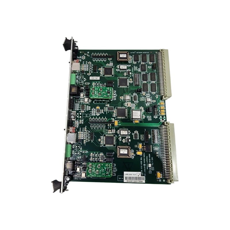
The LAM Research 6004-0100 605-707109-012 is an ultra-high-purity dielectric core component of the process kit specially designed for the upper electrode system of the reaction chamber in semiconductor plasma etching equipment. Serving as a critical coupling connector between the gas showerhead and the electrode backing plate (gas box), or acting as a boundary/focus ring for the plasma confinement zone in the upper chamber area, this part plays an indispensable role in Lam Research etching tools.
Distinct from conventional quartz or ceramic gaskets, the 605-707109-012 is a high-precision functional structural component manufactured through sophisticated material formulation, micron-level mechanical tolerance control, and ultra-clean surface treatment processes. It delivers dual core functions for semiconductor etching processes. Firstly, it provides an extremely flat and stable mounting reference plane for the upper electrode of the reaction chamber, ensuring uniform axial distribution of RF electric fields inside the chamber. Secondly, as a dielectric boundary, it modulates plasma sheath thickness and restricts high-energy ions to bombard the wafer surface vertically, optimizing the anisotropy of the etching profile.
For advanced processes including high-aspect-ratio (HAR) etching in 3D NAND devices and gate etching for FinFET transistors, the geometric precision and material purity of this component are decisive to maintaining etching selectivity and enabling critical dimension (CD) scaling control. Model 605-707109-012 belongs to the customized process kit series for specific Lam Research chamber models and is classified as a periodic consumable spare part with a replacement cycle defined by RF hours or process run counts.
Fabricated from high-purity, high-density, high-strength advanced ceramics (such as high-purity alumina Al₂O₃ and silicon nitride Si₃N₄) or specially doped silicon-based materials, the component features finely polished and laser-textured surfaces to maximize RF coupling efficiency. As the core physical boundary integrating gas distribution, RF energy feeding, and vacuum environment maintenance, it fundamentally determines the initial process gas distribution and profoundly affects plasma density and electron temperature distribution within the chamber. Whether for initial process development of new etching tools or frequent preventive maintenance (PM) in wafer fabs to ensure process consistency and yield stability, this product provides essential upstream hardware support for stable and repeatable advanced semiconductor manufacturing processes.
Product Specifications
|
Parameter Name
|
Parameter Value
|
|
Product Model
|
LAM Research 6004-0100 605-707109-012
|
|
Manufacturer
|
Lam Research
|
|
Product Type
|
Upper chamber dielectric process kit component (coupling ring / showerhead mounting ring / confinement ring)
|
|
Base Material
|
High-purity alumina (Al₂O₃, purity > 99.6%) or high-purity silicon nitride (Si₃N₄)
|
|
Material Density
|
> 3.9 g/cm³ (ensures compact structure and reduces particle generation)
|
|
Relative Dielectric Constant
|
9.0 ~ 10.0 (@ 1MHz, typical for Al₂O₃)
|
|
Dielectric Loss Tangent (tan δ)
|
< 0.001 (minimizes RF energy loss)
|
|
Mounting Surface Roughness
|
Ra < 0.4 μm (ensures vacuum tight fitting with metal backing plate)
|
|
Plasma-Side Surface Roughness
|
Ra 0.8 ~ 1.6 μm (custom textured for optimized gas distribution)
|
|
Geometric Tolerance (Flatness)
|
< 20 μm (full diameter range)
|
|
Operating Temperature Range
|
Room temperature to 400°C (adaptable to chamber high-temperature baking environment)
|
|
Flexural Strength
|
> 300 MPa (guarantees structural integrity under mechanical mounting stress)
|
|
Coefficient of Thermal Expansion
|
6.5 ~ 8.0 × 10⁻⁶ /°C (thermally matched with mating metal components)
|
|
Applicable Gas Environment
|
Fluorine/chlorine/bromine-based plasma (CF₄, NF₃, Cl₂, HBr, etc.)
|
|
Packaging Cleanliness Class
|
Class 1, double-layer vacuum sealed packaging
|
|
Typical Service Life
|
5,000 ~ 15,000 RF Hours (varies with process conditions and plasma power)
|
|
Matching Components
|
Upper gas showerhead, upper electrode backing plate
|
Structure and Composition
The structural design of the LAM Research 6004-0100 605-707109-012 integrates high-precision functional ceramic manufacturing and semiconductor vacuum technology requirements. Geometrically, the component is a large-diameter annular or disc-shaped structure with multiple precision step surfaces and positioning features. Its inner/outer diameter, thickness, and thickness consistency are precisely calculated and strictly controlled to match the mechanical assembly tolerances of the upper electrode in designated reaction chamber models.
The upper surface (facing the electrode backing plate) is engineered with ultra-high flatness and ultra-low surface roughness, minimizing contact thermal resistance and electrical resistance between the component and the metal upper electrode backing plate. Micron-level precision sealing grooves or annular ridges are fabricated on this surface in some versions, which accommodate metal C-rings or form knife-edge sealing structures to confine process gas and cooling gas (e.g., helium) within designated flow channels.
In terms of microstructural materials, the component is fabricated from high-purity ultrafine powder via cold isostatic pressing (CIP) and high-temperature atmospheric/hot-press sintering. It features a dense internal grain structure with extremely low grain boundary phase content, eliminating potential particle sources such as internal pores and microcracks.
Functionally, the plasma-facing lower surface is designed with precisely calculated curved or stepped profiles. Cooperating with the height of the lower electrostatic chuck (ESC), it forms an optimal electric field boundary for the plasma sheath. As a passive functional component with no moving parts, its performance is entirely determined by material dielectric constant, volume resistivity, and dimensional accuracy. It is fixed on the upper electrode backing plate via positioning pins and circumferentially distributed screw holes or pressure rings. Standard cross-sequence torque tightening procedures are mandatory during installation to ensure uniform stress distribution and avoid warpage or deformation.
Key Features and Advantages
1. Ultra-High Material Purity and Minimal Particle Generation
Manufactured with strictly purified high-purity alumina or silicon nitride raw materials, the component controls trace metal impurities (Fe, Na, K, Ni, etc.) below the ppm level. Under long-term high-energy ion bombardment, it avoids introducing harmful metal contaminants into the reaction chamber via sputtering effects. This effectively preserves wafer surface cleanliness and gate oxide integrity (GOI), which is critical for improving the electrical yield of advanced semiconductor devices.
2. High Dimensional Precision and Excellent Process Compatibility
All critical dimensional tolerances including flatness, parallelism, and positioning accuracy are controlled within ±20 microns. This ensures that the plasma discharge gap between the upper and lower electrodes (ESC) can accurately restore the factory baseline after each replacement. Featuring plug-and-play performance, the component eliminates the need for extensive adjustment of RF matching parameters and process recipes after PM maintenance. It significantly shortens post-maintenance process recovery time and ensures continuous and stable production throughput.
3. Superior Thermal Shock Resistance and Extended Service Life
Semiconductor reaction chambers undergo repeated heating, baking, and cooling cycles during production gaps. The advanced ceramic material delivers a high thermal shock resistance coefficient, maintaining complete structural stability without microcracks or edge chipping under drastic temperature gradient changes. Its dense microstructure provides excellent resistance to chemical erosion by fluorine and chlorine-based plasma, slowing surface corrosion. This extended service life helps wafer fabs meet stringent process window requirements while reducing annual spare part consumption and overall operating costs.
Application Fields
The LAM Research 6004-0100 605-707109-012 is mainly applied to high-end plasma etching processes for 200mm and 300mm wafers, serving as a core part of the upper electrode process kit for Lam Research 2300 series etching tools, including Kiyo series dielectric etchers, Flex series conductor etchers, and Exelan series metal etchers.
Its application scope covers anisotropic dielectric etching for logic chip manufacturing (such as silicon oxide spacer and silicon nitride hard mask etching), fine profile definition of polysilicon gates, and low-k dielectric etching in BEOL metal interconnect layers. In memory chip manufacturing, it is widely used in ultra-high-aspect-ratio channel hole etching for 3D NAND flash and deep trench etching for DRAM capacitors. By stabilizing upper electrode electric field distribution and ensuring uniform initial process gas dispersion, it achieves highly consistent structural morphology across the entire wafer surface for HAR etching features.
Beyond core wafer fabrication, the component is also applicable to advanced packaging and MEMS manufacturing processes, including TSV etching and deep reactive-ion etching (DRIE). It effectively solves common process defects caused by upper electrode aging and assembly gap anomalies, such as plasma instability, etching rate drift, and micro-short circuits induced by particle shedding. As a key spare part for chamber maintenance (CM) and new process window evaluation, it is essential for maintaining stable process baselines in advanced wafer fabs worldwide.
Related Products
- LAM Research 605-707109-011: Predecessor model with minor differences in surface roughness and chamfer dimensions. Mixed installation with the -012 model in a single chamber is prohibited; full kit replacement is required.
- LAM Research 605-707109-013: Enhanced version of the same series, designed for high-power and aggressive process recipes, optionally adopting aluminum nitride (AlN) with superior thermal conductivity.
- LAM Research 6004-0100 605-707108-012: Matching lower edge/focus ring for the same chamber, forming a complete upper and lower electric field correction system with the 605-707109-012 component.
- LAM Research 830-101215-101: Special high-purity ceramic positioning pins for precise alignment between the 605-707109-012 and the upper electrode backing plate.
- LAM Research 830-101520-010: High-purity Helicoflex C-type metal seal ring for the interface between the component and metal backing plate, preventing leakage of cooling and process gas.
- LAM Research 6004-0100 605-707109-000: Complete upper electrode assembly kit including the -012 component, sealing parts, and fasteners for full-scale PM replacement.
- LAM Research 810-107813-107: Matched lower gas panel mass flow controller (MFC) that supplies process gas distributed through the showerhead supported by the 605-707109-012 component.
Installation and Maintenance
Pre-Installation Preparation
Before installing the LAM Research 6004-0100 605-707109-012, confirm the reaction chamber has returned to atmospheric pressure, cooled down to room temperature (or the factory-specified safe opening temperature), and been fully purged with nitrogen to eliminate residual toxic and harmful gases. Operators must wear full cleanroom protective equipment, including cleanroom garments, face shields, and nitrile gloves, and perform all operations in a Class 1 microenvironment.
Handle the new component by its edges with clean gloves to avoid direct contact with the plasma-facing surface and sealing surface. Clean the positioning and sealing areas of the upper electrode backing plate with lint-free wipes soaked in electronic-grade isopropanol, followed by high-purity nitrogen blow drying. Place the component horizontally and slowly into position according to alignment marks. Fasten mounting screws to the specified torque value using a calibrated torque wrench in strict accordance with Lam’s official cross-symmetric step-tightening sequence.
Maintenance Guidelines
As a periodic consumable part, its replacement cycle must be formulated strictly based on process RF hour accumulation or wafer processing counts. During each replacement, inspect the surface condition of the upper gas showerhead and the flatness of the lower electrostatic chuck (ESC) to optimize the overall matching state of chamber components.
Examine old components for surface discoloration, microcracks, or erosion pits during removal. These anomalies usually correlate with corrosive process recipes or abnormal chamber discharge, requiring timely recording and process parameter evaluation. Waste components must be recycled in compliance with fab hazardous waste management regulations for toxic and heavy-metal-containing materials.
After installation, conduct chamber bake-out treatment and no less than one dummy wafer etching cycle for surface seasoning. Mass production wafer processing can only be resumed after key process parameters (etching rate, reflected power, etc.) stabilize completely.