Product Overview
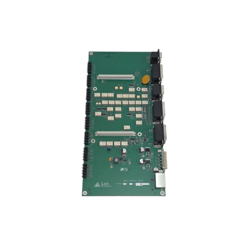
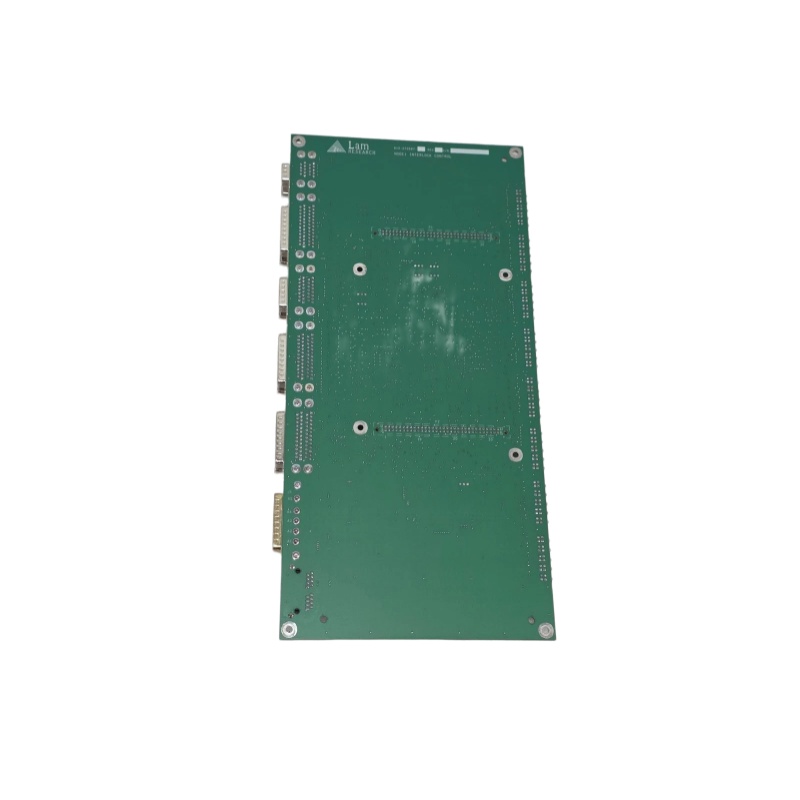
The Lam Research 810-072687-410 is a high-performance Printed Circuit Board Assembly (PCBA) developed by Lam Research, specifically designed for the company’s semiconductor plasma etching and deposition equipment systems. Classified as an RF PCBA (Radio Frequency Printed Circuit Board Assembly), this component focuses on the generation, conditioning, distribution, and monitoring of critical signals within the equipment’s radio frequency system.
In semiconductor manufacturing processes, RF energy serves as the core power source for generating and sustaining plasma. The quality of RF energy directly determines key process metrics, including etching rate, process uniformity, and wafer surface damage. Accordingly, the stable and precise operation of the Lam Research 810-072687-410 is one of the essential elements for ensuring plasma process stability and improving wafer yield.
This board is designated as a Non-RC (Non-Resistor-Capacitor) type, a technical specification indicating that its RF circuit design adopts a specialized architecture distinct from conventional simple RC networks. Its internal structure integrates active devices, dedicated matching networks, and sophisticated signal processing functions. As an original genuine and high-value spare part certified by Lam Research, the 810-072687-410 strictly complies with global semiconductor industry standards in design, material selection, and manufacturing. It delivers long-term and reliable performance under the extreme operating conditions of semiconductor fabs, including high frequency, high power, and strong electromagnetic interference, acting as an indispensable hardware foundation for the efficient production of advanced logic and memory chip production lines.
Product Specifications
|
Parameter Name
|
Parameter Value
|
|
Product Model
|
810-072687-410
|
|
Manufacturer
|
Lam Research
|
|
Product Type
|
RF Printed Circuit Board Assembly (RF PCBA)
|
|
Technical Features
|
Non-Resistor-Capacitor (Non-RC) Type
|
|
Functional Positioning
|
RF signal generation, conditioning and monitoring
|
|
Hardware Version
|
Rev. A01 and other compatible versions
|
|
Compatible Platforms
|
Lam Research semiconductor etching and deposition equipment
|
|
Application Environment
|
Class 1000 or higher cleanroom / Semiconductor Fab environment
|
|
Product Status
|
Spare part / Replacement part
|
Structure and Composition
The internal structure of the Lam Research 810-072687-410 embodies the core design principles of high-frequency, high-reliability RF circuit boards. It is a multi-layer PCB fabricated with high-quality microwave substrates (such as Rogers RO4000 series or equivalent high-performance materials). These substrates feature extremely low dielectric loss and frequency-stable dielectric constant, laying a solid foundation for maintaining complete RF signal integrity.
The board is divided into multiple independent functional areas, mainly including an RF signal input/output interface unit, a signal conditioning and matching network, and a monitoring and diagnosis circuit.
The RF signal input/output interface unit adopts professional RF coaxial connectors (such as SMA, BNC, or customized connectors) to connect the system’s RF source (RF generator) and load (plasma chamber). As the core functional area of the board, the signal conditioning and matching network consists of high-Q inductors, capacitors, and microstrip line-based impedance matching circuits, as well as passive and active power distribution/combination networks. It efficiently transmits the output power of the RF generator to the plasma chamber with minimal reflection loss.
The monitoring and diagnosis circuit integrates precision components such as directional couplers and peak detectors to collect real-time sampling signals of forward and reflected power. It provides critical data for equipment matching tuning and arc fault detection. All functional units work collaboratively to form a complete and high-precision RF signal link node.
Key Features and Advantages
1. Excellent RF Performance and Signal Integrity
Optimized exclusively for semiconductor plasma process applications, the Lam Research 810-072687-410 achieves ultra-low insertion loss and high phase consistency within mainstream operating frequency bands (including 2MHz, 13.56MHz and higher frequencies). Its precision-engineered impedance matching network ensures efficient RF power transmission from the generator to the chamber, minimizing energy waste and equipment damage risks caused by reflected power. This performance is critical for achieving high and stable etching rates while reducing process-induced wafer damage.
2. High Reliability and Ruggedized Design
Tailored for the 24/7 long-term high-load continuous operation of semiconductor equipment, the board adopts a redundant and margin-rich design scheme. All internal RF power devices and passive components are industrial-grade or military-grade products with high rated parameters. The PCB substrate features a high glass transition temperature (TG) and low coefficient of thermal expansion (CTE), maintaining dimensional stability and reliable electrical connection under temperature fluctuations caused by high RF power, thus greatly extending the service life of the component.
3. Modular Architecture and Accurate Fault Location
The 810-072687-410 adopts a modular design and serves as an independently replaceable functional unit in the RF link. When RF system-related faults occur (such as high reflected power, tuning failure, and arc alarm), this board acts as a key detection point for fault isolation. Its on-board monitoring circuit provides engineers with real-time and accurate RF parameter data to assist in rapid fault source localization. Once a board failure is confirmed, its modular design reduces the Mean Time To Repair (MTTR) from several hours to mere minutes, significantly improving equipment uptime.
Application Fields
The Lam Research 810-072687-410 is applied in the core processes of semiconductor chip manufacturing: plasma etching (Etch) and Plasma-Enhanced Chemical Vapor Deposition (PECVD). It is integrated into Lam Research’s mainstream equipment platforms, including the 2300®, Kiyo®, and Versys® series etching and deposition systems, and widely used in the production of logic chips (CPU, GPU), memory chips (DRAM, 3D NAND flash), and partial power devices.
Its core application scenarios are divided into two categories. First, as a core part of the RF matching network, it dynamically adjusts the input impedance of the plasma chamber to match the standard 50Ω output impedance of the RF generator, realizing maximum power transmission. Second, as an RF sensor interface module, it converts high-frequency voltage and current signals on the RF transmission line into low-frequency signals identifiable by the control system, enabling real-time plasma state monitoring and process endpoint detection.
The operating status of the Lam Research 810-072687-410 directly affects wafer etching rate, process uniformity, and critical dimension (CD) stability. For semiconductor fabs, stocking this model is a key strategy to respond to sudden RF system faults and ensure continuous production line operation.
Related Products
- Lam Research 810-072687-xxx: Other RF PCBA models in the same series, with similar core functions but different parameters and configurations, adapting to different RF power levels and frequency ranges.
- Lam Research 810-800256-004 / 005: Node boards of the 810 series, core components of the equipment control system, which work in coordination with RF boards to complete full process control.
- Lam Research 810-707103-001: I/O bus control board, responsible for internal equipment data communication management, belonging to a different functional subsystem from the RF PCBA.
- Lam Research 810-707150-001: Neuron PCB, an underlying signal acquisition and local control module, forming the basic nodes of the equipment distributed control network.
- Lam Research 810-495659-308: Electrostatic Chuck (ESC) power supply and control PCBA, a high-value core spare part matching the RF board in equipment systems.
Installation and Maintenance
Pre-installation Preparation
The installation of the 810-072687-410 must be performed by Lam Research certified professional technicians in a Class 1000 or higher controlled cleanroom environment. Prior to operation, the main equipment power supply must be completely cut off, and the Lockout/Tagout (LOTO) procedure must be implemented to ensure full discharge of the RF generator.
Operators must wear complete cleanroom garments and ESD (Electrostatic Discharge) protective equipment, including ESD wristbands and grounding wires. During installation, align and lock the board with the system via RF and on-board connectors carefully, ensuring complete fitting of coaxial connector center pins and shells. Improper connection will cause poor contact and increased RF reflection. Direct contact with RF transmission lines and components on the board is strictly prohibited to avoid contamination and physical damage that may degrade RF performance.
Maintenance Recommendations
The maintenance of the 810-072687-410 focuses on preventive inspection and equipment log data analysis. During regular maintenance, inspect RF connectors for wear, oxidation, and center pin collapse, and check fastening torque in accordance with official specifications. Conduct visual inspection of the board surface for discoloration and component ablation caused by overheating.
In case of RF-related alarms (such as reflected power over-limit and matcher tuning timeout), the 810-072687-410 shall be prioritized for troubleshooting based on equipment logs. After replacing with a new board, a complete equipment RF calibration procedure is required to match parameters between the new board, matcher and plasma chamber, restoring the equipment to optimal process performance.