Product Overview
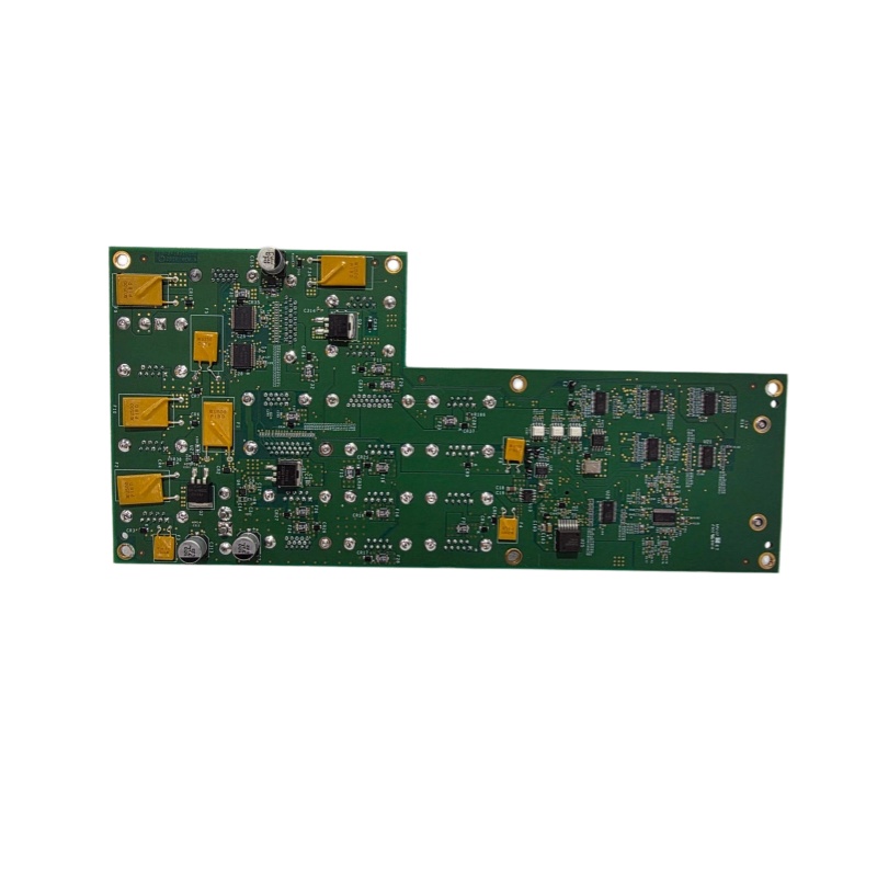
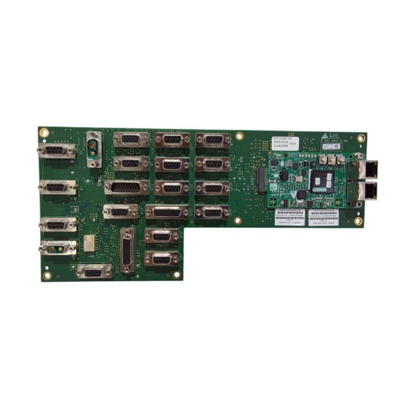
The Lam Research 810-341681-102 is a high-precision Printed Circuit Board Assembly (PCBA) custom-designed by Lam Research for its industry-leading semiconductor plasma etching and deposition equipment. In semiconductor manufacturing processes, RF energy serves as the core power source for generating and sustaining plasma. Minor fluctuations in RF parameters including voltage, current, phase, and power will directly affect critical process indicators such as etch rate, process uniformity, and wafer damage.
Serving as a precise “sensing unit” in the RF transmission chain, the Lam Research 810-341681-102 is engineered to collect high-frequency voltage and current signals from RF transmission lines in real time and with high accuracy. It converts the acquired high-frequency signals into low-frequency, digital signals processable by equipment control systems (e.g., matcher logic controller or mainframe), enabling precise monitoring and closed-loop regulation of plasma states. This sensor board acts as the fundamental hardware guarantee for high-precision RF power control required by advanced semiconductor manufacturing processes.
Product Specifications
|
Parameter Name
|
Parameter Value
|
|
Product Model
|
810-341681-102
|
|
Manufacturer
|
Lam Research
|
|
Product Type
|
RF Sensor Board
|
|
Functional Description
|
Collects RF voltage and current signals to support control system monitoring of plasma status
|
|
Typical Installation Position
|
Integrated inside automatic RF Matching Network
|
|
Compatible Platforms
|
Lam Research semiconductor etching and deposition equipment (e.g., 2300 Series)
|
|
Application Environment
|
Class 1000 or higher cleanroom / Semiconductor Fab environment
|
|
Main Interfaces
|
RF coaxial port, low-voltage signal & power cable harness
|
|
Product Status
|
Spare / Replacement Part
|
Structure and Composition
The internal structure of the Lam Research 810-341681-102 embodies the sophisticated design of high-frequency precision measurement circuits. It is built on a printed circuit board adopting high-performance microwave substrates (e.g., Rogers RO4000 series or equivalent materials). Featuring ultra-low dielectric loss and highly stable dielectric constant, the substrate guarantees superior RF signal integrity and measurement accuracy.
The functional areas of the board are divided into three core units: RF signal coupling and attenuation unit, signal conditioning and detection unit, and digital processing and communication interface unit.
The RF signal coupling and attenuation unit serves as the front-end of the system. It adopts high-precision directional couplers or resistor-capacitor voltage divider networks to safely extract a tiny proportion of voltage and current samples from RF transmission lines and attenuate the signals to safe levels compatible with subsequent circuit processing.
The signal conditioning and detection unit acts as a signal converter. Equipped with precision detectors (e.g., logarithmic detectors, RMS detectors) and high-speed Analog-to-Digital Converters (ADC), it converts coupled RF signals into DC levels or digital values proportional to key parameters such as power and Voltage Standing Wave Ratio (VSWR).
The digital processing and communication interface unit consists of a Microcontroller Unit (MCU) or Complex Programmable Logic Device (CPLD) and peripheral circuits. It is responsible for digital processing, calibration, and data packaging of sampled signals, and transmits real-time measurement data to the matcher main control logic or equipment host via communication buses (e.g., RS-485, SPI). The coordinated operation of the three functional units enables the 810-341681-102 to accurately and real-timely reflect the operating status of the RF link.
Key Features and Advantages
1. High-Precision RF Measurement with Wide Dynamic Range
Optimized exclusively for semiconductor plasma applications, the Lam Research 810-341681-102 maintains excellent measurement linearity and accuracy over a wide RF power dynamic range (typically from several watts to several kilowatts). It precisely captures forward power, reflected power, VSWR, and other critical parameters, providing accurate data input for matcher algorithms. This enables fast and precise impedance matching, minimizing damage to RF generators caused by reflected power and eliminating fluctuations in process stability.
2. Superior Anti-Interference Capability and Measurement Repeatability
Given the harsh electromagnetic environment inside RF matchers with adjacent high-power RF transmission lines, the sensor board is designed with strict Electromagnetic Compatibility (EMC) optimization. It adopts standardized shielding and grounding layouts and high common-mode rejection ratio differential sampling schemes, effectively suppressing external electromagnetic interference on weak sampling signals. The design delivers highly repeatable measurement results, providing a reliable hardware foundation for equipment to quickly restore standard process status after maintenance or component replacement.
3. Modular Design for Improved Maintenance Efficiency
Featuring a modular structure, the board is an independently replaceable functional component inside the RF matcher. For RF monitoring-related equipment abnormalities (e.g., abnormal reflected power readings, slow or failed matcher tuning), the board serves as a priority troubleshooting point for engineers. Once a fault is confirmed, its modular design supports rapid replacement, reducing the Mean Time To Repair (MTTR) from several hours to minutes and significantly improving the Overall Equipment Effectiveness (OEE).
Application Fields
The Lam Research 810-341681-102 is applied to core semiconductor manufacturing processes, including plasma etching and Plasma-Enhanced Chemical Vapor Deposition (PECVD). It is widely deployed on Lam Research mainstream platforms such as the 2300® Series, Kiyo® Series, and Versys® Series for the manufacturing of logic chips (CPU, GPU), memory chips (DRAM, 3D NAND flash), and partial power devices, functioning as a key internal component of automatic RF matchers.
Its core application scenarios are summarized as follows: First, it provides feedback input for the matcher closed-loop control system, delivering real-time forward and reflected power data to drive stepper motors or variable reactance components in the matching network and dynamically adapt to chamber load changes. Second, it acts as a process diagnosis and monitoring tool, transmitting real-time RF parameter data streams to the equipment control system for plasma status monitoring, process endpoint judgment, and preventive maintenance (PM) cycle decision-making. A fully functional 810-341681-102 ensures fast matcher response, stable etch rate, and consistent process results.
Installation and Maintenance
Pre-Installation Preparation
The installation of the 810-341681-102 must be performed by Lam Research certified professional technicians in a Class 1000 or higher controlled cleanroom environment. Before operation, cut off the main equipment power supply and RF generator output, and complete the Lockout/Tagout (LOTO) procedure to ensure full discharge of energy storage components inside the matcher. Operators must wear complete cleanroom garments and anti-static protective equipment.
The board is installed inside the matcher chassis. During installation, carefully remove the matcher outer casing, connect the new board to the corresponding internal interfaces via RF coaxial connectors and low-voltage cable harnesses. Ensure intact center pins of coaxial connectors, compliant fastening torque, and firm, correct-direction cable connection. Direct contact with RF transmission lines and precision components on the board is strictly prohibited.
Maintenance Recommendations
Daily maintenance of the 810-341681-102 focuses on equipment log analysis and preventive inspection. During regular matcher maintenance, visually inspect the board for dust accumulation, discoloration, or component damage, and check all connectors for looseness and oxidation.
In daily equipment monitoring, systematic deviation of reflected power readings, increased signal noise, or significantly slowed matcher response without physical faults indicate potential failures of the sensor board, which should be prioritized for inspection. After board replacement, perform standard matcher calibration procedures in accordance with the official equipment manual to align the measurement benchmark of the new sensor board with system software and restore the equipment to optimal tuning and process status.